portfolio, case studies, and engineering work
electrical engineering / physical design
Analog Front-End Layout & Verification
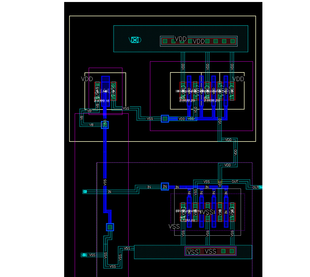
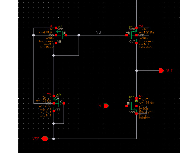
I took a common-source CMOS amplifier through the full custom IC flow, ending with DRC, LVS, PEX, and post-layout validation in TSMC 65 nm.
recruiter case study
- Executed the complete Virtuoso-to-Calibre flow: schematic capture, symbol generation, testbenching, layout drafting, DRC, LVS, PEX, and post-layout simulation.
- Used schematic-driven layout plus manual place-and-route to keep interconnect short and parasitics controlled on TSMC 65 nm design rules.
- Compared pre- and post-layout behaviour directly, treating layout as an electrical design problem rather than a final documentation step.
stack
evidence
role
physical design and verification owner for the analog block layout and post-layout checks.
problem
The challenge was to preserve amplifier behaviour through layout while staying clean on all foundry checks and minimizing routing parasitics.
ownership
I handled schematic-driven layout, manual place-and-route, DRC/LVS closure, and post-layout comparison against the original design intent.
outcome
Closed DRC with no true rule violations, passed LVS with a full match, completed PEX successfully, and measured the midband gain drop from about 12 V/V pre-layout to about 10-11 V/V post-layout as the extracted parasitics shifted the dominant pole lower.
artifact
Full layout-verification report with final layout captures, DRC/LVS/PEX screenshots, extracted-view confirmation, and pre/post-layout AC, DC, and transient results.
Full layout report and supporting common-source files are available above.