portfolio, case studies, and engineering work
electrical engineering / mixed-signal ic design
Mixed-Signal ECG Front-End IC
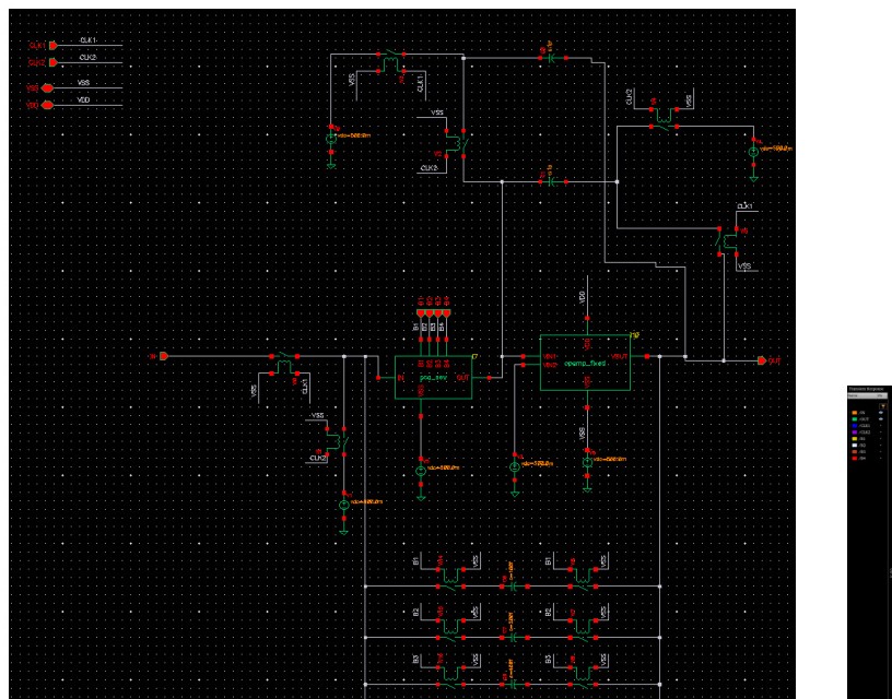
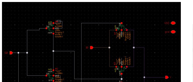
I designed a smartwatch-oriented ECG front-end in TSMC 65 nm that combined a 3:1 CMOS mux, switched-cap PGA, and 6-bit SAR ADC under a 1 V supply.
recruiter case study
- Designed around a realistic smartwatch constraint set: 1 V battery supply, 20 mV maximum ECG amplitude, 10 kΩ source resistance, and low-power operation on TSMC 65 nm CMOS.
- Integrated the analog path end-to-end, including the 3:1 mux, switched-cap PGA with gains of 1 through 4, a two-stage CMOS op-amp, and a 6-bit SAR ADC with Verilog-A control logic.
- Verified the chain at block and top level using DC, AC, and transient simulation, then documented the design as a full ENGG 4080 mixed-signal project report.
stack
evidence
role
mixed-signal designer responsible for the analog front-end architecture, transistor-level implementation, and simulation/verification path.
problem
The design had to resolve low-amplitude ECG signals around a 0.5 V common-mode level, provide programmable gain, and convert the output on-chip under a strict 1 V supply and low-power budget.
ownership
I designed the mux, the switched-cap PGA, the two-stage op-amp, the comparator path, the binary-weighted capacitor array, and the Verilog-A SAR control used to drive conversion.
outcome
The design met the main project targets: about 40 dB open-loop op-amp gain, measured PGA gains of 1x to 4x within roughly 5-10% of ideal, a 6-bit ADC with 15.625 mV LSB and at least 105 samples/s, and expected analog front-end power well below 100 µW.
artifact
Full ENGG 4080 report with block diagrams, op-amp AC results, PGA gain stepping waveforms, top-level ADC simulation, and the Verilog-A SAR listing.
Full mixed-signal report and related analog lab files are available above.